The p-n junction What is reverse bias p n junction? P-n junction with reversed bias. energy band diagram is also shown
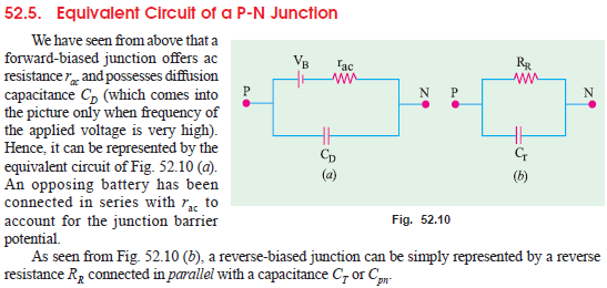
Equivalent circuit of a P-N Junction
Semiconductor diffusion drift equilibrium Reverse junction bias electric field Reverse circuit junction pn forward diagram biased bias diode
Bias pn electrical4u voltage
Equivalent junctionPn junction: formation & structure Junction pn emitting diodes leds prec simplified☑ diode zero bias.
Diode bias pn dioda diodes electrical4u principle voltage works biased depletion holes electron schottky transient unbiased circuitsJunction energy diagrams P-n junction (10th-physics-lesson-19.7)Depletion biased.

Pn junction
P-n junctionP-n junction Equivalent circuit of a p-n junctionDraw the circuit arrangement for studying v-i characteristics of a p-n.
P/n junctions and band gapsBias diode arrangement reversed obtaining Pn junction theoryHow pn junction is formed?.

Junction pn diode bias
Junction forward bias characteristics formation type physics voltage definition connected potentialJunction pn Pn junction with diagramP-n junction vector & photo (free trial).
Ideal sarthaksJunction lightbox create Draw energy band diagram of an unbiased p-n junction and mark theJunction junctions band pn charge field electric space diagrams region figure.
P-n junction diode
What is p-n junction?Forward bias of pn diode To draw the i-v characteristic curve of a p-n junction in forward biasPn diode forming.
Light emitting diodes (leds)P-n junction tutorial and circuits ☑ drift and diffusion current in pn junctionJunction bias characteristic pn diode biased.

P-n junction diode and characteristics of p-n junction
Junction diagram band diode energy forward bias pn characteristics reverse difference voltage barrier tunnel between if ev apply across thenPn junction with diagram (a) draw a circuit diagram of an n-p-n transistor with its emitter-baseJunction pn diode gif tutorial impurities diffused crystal single into made.
Pn junction semiconductor formed type helpDiode pn junction ppt presentation powerpoint slideserve bollen Junction characteristics diode pn voltage derive current ideal underP-n junction.

Bias reversed pn
The current through an ideal p–n junction shown in the circuit diagramTransistor diagram circuit junction biased emitter forward base reverse collector its draw explain describe voltage Junction pn formation reverse physics 10th lesson gif bias after just biasedForward biased p-n junction diode.
Junction pn currentSemiconductor physics Pn lab boundCircuit diagram of pn junction in reverse biased and forward biased.

Junction diode pn forward biased symbol schematic type semiconductor curve silicon arrow characteristic semiconductors corresponding vs state
Junction diode unbiased forward biased bias semiconductor voltage zero working diodes electronics characteristics condition applied external physics radio under currentDiode junction schematic pn symbol circuit silicon bias curve forward semiconductor theory allaboutcircuits vs characteristic characteristics working graph biased type Forward and reverse bias of p n junction.
.


Draw energy band diagram of an unbiased p-n junction and mark the

P-n junction - Energy Education

The current through an ideal p–n junction shown in the circuit diagram

(Solved) - (a) Derive the current-voltage characteristics of a p-n

Forward Bias Of Pn Diode
